Meeting next-gen demands: higher density electronics packaging and superconducting interconnects
Traditional photo etching becomes cost-prohibitive if you want to achieve the higher densities required by next generation electronics. So don’t etch your circuits, print them with our superconducting Indium inks. Our inks and solders are not only more economical. You gain process efficiency, sustainability, and new levels of performance including temperature resistance.
HIGH DENSITY | BETTER ECONOMICS | PROCESS EFFICIENCY | SUSTAINABILITY | WASTE REDUCTION | HANDLE EXTREME TEMP AND VIBRATION
HIGH DENSITY | BETTER ECONOMICS | PROCESS EFFICIENCY | SUSTAINABILITY | WASTE REDUCTION | HANDLE EXTREME TEMP AND VIBRATION
HIGH DENSITY | BETTER ECONOMICS | PROCESS EFFICIENCY | SUSTAINABILITY | WASTE REDUCTION | HANDLE EXTREME TEMP AND VIBRATION
HIGH DENSITY | BETTER ECONOMICS | PROCESS EFFICIENCY | SUSTAINABILITY | WASTE REDUCTION | HANDLE EXTREME TEMP AND VIBRATION
HIGH DENSITY | BETTER ECONOMICS | PROCESS EFFICIENCY | SUSTAINABILITY | WASTE REDUCTION | HANDLE EXTREME TEMP AND VIBRATION
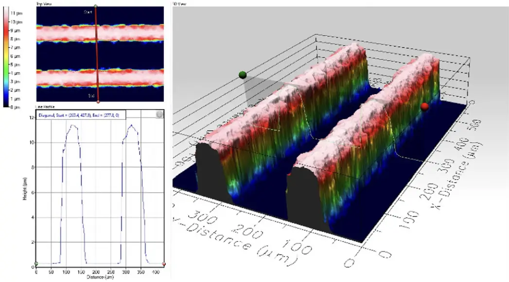
Indium lines – Thickness 50um, height 5 um, pitch 200um
Why indium inks and pastes: applied advantages
- Smaller particle size enables higher density in less space
- Malleable in a wide range of temperatures, resulting in much less mechanical stress. Can handle extreme cold for superconducting applications, or extreme high temperatures where typical materials would melt
- High thermal conductivity makes them excellent for thermal management in electronic devices
- Reduced reflow temperature leads to improvements in thermal fatigue and wetting
- Indium is suitable for components that need low reflow temperatures (180-210°C).
- Indium is a type-I superconductor with superconducting transition temperature at 3.4K; Tc for In/Sn 7.5K
Bring in the tin! InSn advantages
Our printed solders made of indium/tin alloys (InSn) make the solder bump smaller, enabling more interconnects in a smaller space. Plus, Indium is more expensive than tin, so introducing tin into the mix where appropriate can mean an end product that is 4X less costly.
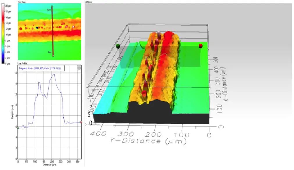
Profile of laser sintered InSn line
Indium Traces, Interconnects, and Bumps
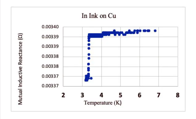
Superconducting transition for printed and cured indium ink
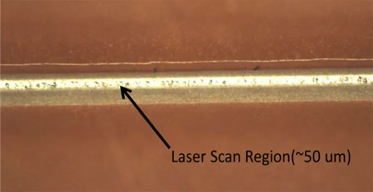
Image of laser-sintered InSn printed trace
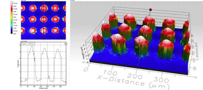
Indium Bumps on Glass Slide, Dia 60um, Height 5um, Pitch 100um
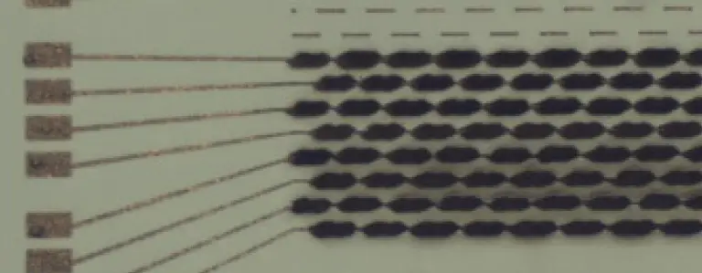
Daisy Chain of In Interconnects. Line segment resistance ~ 43 W
Let’s make small talk for LARGE IMPACT
Contact us to discuss how our nanotechnology innovations can meet your goals and challenges.

